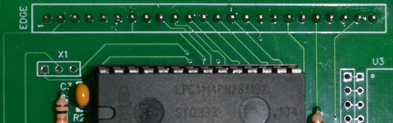
At some point in every electronics hobbyist’s life, there comes a dramatic moment: you are hunched over a copper-clad board, squinting like a jeweler, inhaling suspicious fumes, and asking yourself, “Why am I still making PCBs by hand when a board house can ship me ten shiny purple, green, black, or blue beauties for the price of a mediocre lunch?”
It is a fair question. Printed circuit boards, or PCBs, are the backbone of modern electronics. They hold components, connect signals, organize power, reduce wiring chaos, and make a project look less like a bowl of electronic spaghetti. Today, professional PCB fabrication is cheaper, faster, and more accessible than ever. You can design a circuit in KiCad, EasyEDA, Altium, Eagle, or another PCB design tool, export Gerber files, upload them to a manufacturer, and wait for a neat little stack of boards to arrive.
So why are people still making PCBs at home? Why do makers still etch boards in garages, mill copper on desktop CNC machines, cut jumper wires on perfboard, or solder prototypes onto stripboard like tiny electronic quilts? The answer is not simply “because they enjoy pain,” although anyone who has debugged a bad via at midnight may suspect otherwise.
The real answer is more interesting: making PCBs is still useful, educational, creative, and sometimes faster than outsourcing. But it is no longer the only pathor even the best pathfor every project. The smart approach is knowing when to make a PCB yourself and when to let a professional PCB fabrication service do the heavy lifting.
What Does “Making PCBs” Actually Mean?
When people say they are “making PCBs,” they may mean several different things. One person might be designing a custom printed circuit board and sending it to a manufacturer. Another might be chemically etching copper at home. A third might be using a desktop CNC mill to remove unwanted copper from a blank board. Someone else might be assembling a circuit on perfboard and calling it “close enough,” which is the official slogan of many first prototypes.
A printed circuit board is a physical platform that uses copper traces, pads, vias, solder mask, silkscreen, and insulating substrate to connect electronic components. Instead of running individual wires between every resistor, IC, capacitor, connector, sensor, and microcontroller pin, the PCB routes those connections in a compact, repeatable layout.
In a professional PCB manufacturing workflow, you usually begin with a schematic, convert it into a board layout, define design rules, route traces, check clearances, generate Gerber files and drill files, and send the package to a fab house. For assembled boards, you may also provide a bill of materials, pick-and-place file, assembly drawing, and sometimes a stencil file for solder paste.
In a DIY workflow, the steps can be rougher. You may print artwork, transfer toner to copper, etch away unwanted copper with chemicals, drill holes manually, and solder everything by hand. It can feel like science class, shop class, and a mild plumbing emergency all at once.
Why People Stopped Making PCBs by Hand
Professional PCB fabrication became affordable
Years ago, ordering a custom PCB felt like something only companies, universities, or extremely committed engineers could justify. Setup fees were painful, lead times were long, and small orders were not always friendly to hobbyists. Today, the situation has changed dramatically. Prototype PCB services have made small-batch board production available to students, startups, repair technicians, makers, and weekend inventors.
Many PCB manufacturers now offer instant quotes, online Gerber viewers, low-cost two-layer boards, multiple solder mask colors, surface finishes like HASL or ENIG, and optional stencil or assembly services. For a small design, it is often cheaper to order a batch than to buy fresh chemicals, copper-clad laminate, drill bits, transfer paper, and a replacement sense of patience.
Quality is better and more consistent
A professionally made PCB can include plated through-holes, fine trace widths, accurate drill registration, solder mask, silkscreen labels, controlled board thickness, consistent copper weight, and clean edges. Those features are hard to reproduce at home without specialized tools.
Solder mask alone is a quiet hero. It protects copper, reduces accidental solder bridges, improves assembly, and makes the board look finished. Silkscreen labels help you identify components and connectors without playing “guess that resistor footprint” after your third cup of coffee.
Modern components demand precision
Through-hole parts are forgiving. Large DIP chips, chunky resistors, and screw terminals are happy to live on perfboard. But modern electronics increasingly use surface-mount components, fine-pitch ICs, QFN packages, tiny passives, USB-C connectors, RF modules, and dense microcontroller boards. These parts are not impossible to solder by hand, but they are much easier to work with on a professionally fabricated PCB.
If your design uses narrow trace spacing, controlled impedance, multi-layer routing, ground planes, high-current paths, differential pairs, or thermal reliefs, professional PCB fabrication is usually the sensible route. A home-etched board may technically work, but “technically” is doing a lot of heavy lifting in that sentence.
Why People Still Make PCBs Anyway
Speed matters when inspiration is hot
Ordering PCBs is convenient, but it is not instant. Even fast-turn boards require manufacturing time and shipping. If you need to test a simple circuit today, a breadboard, perfboard, stripboard, or milled PCB can beat waiting for delivery.
This is especially true during early prototyping. If you are testing whether a sensor talks to a microcontroller, whether a power supply behaves, or whether a connector pinout is correct, a quick handmade prototype can save days. The first version of a circuit is often not the final version anyway. It is more like a rough draft with electrons.
Learning PCB design by touching the process
Making a PCB by hand teaches lessons that software tutorials often skip. You learn what copper actually looks like. You understand why trace width matters. You discover that drilling tiny holes by hand is a character-building activity. You develop a deep, personal relationship with continuity testing.
When you physically create a board, you become more aware of real-world constraints: component spacing, pad size, heat, solder flow, oxidation, mechanical stress, and the difference between “the schematic is correct” and “this board can actually be assembled by a human with normal-sized hands.”
DIY boards are useful for one-off experiments
Not every circuit deserves a full professional manufacturing cycle. A quick LED driver, test jig, breakout adapter, programming header, audio filter, sensor interface, or power distribution board may only be needed once. In those cases, making a PCB yourself can be practical.
Engineers and makers often build small support boards that never become products. They exist to answer a question, test a part, adapt a connector, or rescue a project from a wiring disaster. For these temporary jobs, “good enough” is not an insult. It is a design specification.
Creative control is addictive
There is also the simple joy of making. Some people bake bread even though grocery stores exist. Some people build furniture even though chairs are not exactly endangered. In the same spirit, some people make PCBs because the process itself is satisfying.
PCB design can be practical art. Trace routing has rhythm. Component placement has balance. Silkscreen can be functional, funny, or beautiful. A well-designed board feels like a tiny city where every road has a purpose and every component has a place to park.
When You Should Stop Making PCBs Yourself
When reliability matters
If the board will go into a customer product, medical device, automotive system, industrial controller, safety-related circuit, or anything that could cause harm if it fails, do not rely on a casual handmade PCB. Professional fabrication, design review, assembly control, testing, and documentation matter.
Reliability is not just about whether the board works on your bench once. It is about whether it works after vibration, heat, cold, humidity, repeated plugging and unplugging, manufacturing variation, and the mysterious behavior of users who can break anything by “just trying it normally.”
When the design needs repeatability
Handmade boards are charming, but they are not always repeatable. A slight over-etch, under-etch, drill misalignment, incomplete transfer, solder bridge, or hairline copper defect can create failures that are difficult to reproduce and even harder to explain.
If you need five, ten, fifty, or five hundred identical boards, use a PCB fabrication service. Repeatability is one of the biggest reasons PCBs exist in the first place.
When assembly is complex
A board with a few resistors and headers is easy to assemble at home. A dense surface-mount board with dozens of tiny components, fine-pitch ICs, multiple voltage rails, and a USB-C connector that looks like it was designed by a committee of watchmakers is another story.
Professional PCB assembly services can handle solder paste application, pick-and-place, reflow, inspection, and sometimes functional testing. You still need to design the board carefully, choose available parts, verify footprints, and review the assembly files, but you do not need to hand-place every 0402 capacitor while questioning your life choices.
When Making Your Own PCB Still Makes Sense
Use DIY methods for fast learning
If you are learning electronics, making a simple PCB can be a fantastic exercise. Start with a basic circuit: an LED flasher, small audio amplifier, sensor breakout, motor driver, or microcontroller shield. Keep the traces wide, the components large, and the layout simple.
The goal is not to beat a professional board house. The goal is to understand the path from schematic to physical circuit. Once you have seen that process up close, professional PCB design starts to feel less mysterious.
Use perfboard for quick permanent builds
Breadboards are great for temporary testing, but they are not ideal for long-term use. Jumper wires come loose, contacts wear out, and vibrations can turn a working project into a tiny haunted house.
Perfboard and stripboard offer a middle ground. They are more permanent than breadboards but faster than a custom PCB. For simple circuits, test fixtures, workshop tools, and one-off builds, they are still incredibly useful.
Use desktop PCB milling for same-day prototypes
Desktop PCB milling removes copper mechanically instead of using chemical etching. It can create simple boards quickly and avoids wet chemistry. It is useful in classrooms, labs, hackerspaces, and workshops where rapid iteration matters.
However, milled boards usually lack plated through-holes, solder mask, and silkscreen unless additional steps are added. Fine-pitch work can be challenging, tool wear matters, and board flatness can make or break the result. It is a great method, but not magic. Like all shop tools, it rewards patience and punishes optimism.
PCB Design Is More Than Routing Traces
Whether you make a board yourself or order it, good PCB design starts before layout. The schematic must be correct. The components must be available. The footprints must match the actual parts. Connectors must face the right direction. Mounting holes should line up with the enclosure. Power traces need to handle current. Ground return paths should make sense.
This is where design for manufacturing, often called DFM, becomes important. DFM means designing the PCB so it can be fabricated, assembled, inspected, and tested without unnecessary problems. It includes clearance rules, trace widths, annular rings, solder mask expansion, drill sizes, copper balance, panelization, component spacing, thermal reliefs, and documentation.
A beautiful PCB layout that cannot be manufactured is not a design. It is modern art with a bill of materials.
Common Mistakes That Make PCB Projects Painful
Trusting footprints without checking them
A wrong footprint is one of the classic PCB disasters. The schematic looks perfect. The board arrives. Then you discover the connector pins are mirrored, the regulator package is wrong, or the push button footprint fits a part that only exists in a parallel universe.
Always compare the footprint against the datasheet. Print the board layout at 1:1 scale and place real components on the paper if possible. It feels old-school, but it catches mistakes that expensive software will politely allow you to make.
Skipping design rule checks
Design rule checks exist because humans are creative, tired, and easily betrayed by grids. Run electrical rule checks on the schematic and design rule checks on the PCB layout. Check clearances, unconnected nets, overlapping pads, missing pours, silkscreen over pads, and drill sizes.
A few minutes of checking can prevent a week of staring at a board and whispering, “But it worked in my head.”
Ignoring test points
Every prototype should include places to measure important signals. Add test points for power rails, ground, reset, programming lines, communication buses, sensor outputs, and anything you might need during debugging.
Test points are cheap when you design them in. They are expensive when you are trying to hold a multimeter probe on the leg of a tiny IC while your other hand presses reset and your third hand, which you sadly do not have, types commands into a terminal.
The Best Modern Workflow: Prototype Smart, Fabricate Smarter
The best answer to “Why are you still making PCBs?” is not “always stop” or “always continue.” The best answer is to choose the right method for the job.
Use a breadboard when the circuit is simple, low-frequency, and temporary. Use perfboard when you need something more permanent but not worth a custom layout. Use a homemade or milled PCB when speed, learning, or experimentation is the priority. Use professional PCB fabrication when you need precision, repeatability, solder mask, silkscreen, plated holes, smaller components, or multiple copies.
For many makers and engineers, the winning workflow looks like this: test the concept on a breadboard, build a rough permanent version on perfboard if needed, design a proper PCB, order a small batch, test thoroughly, revise the design, then order the improved version. That process may sound slow, but it is much faster than pretending version one will be perfect. Version one is not perfect. Version one is a polite suggestion from your future self.
Experience Section: Lessons From the Bench
The first time you make a PCB, you usually learn two things. First, electronics is wonderfully logical. Second, the physical world is a prankster. A schematic can be correct and still become a frustrating board if the layout ignores heat, routing, mechanical fit, or assembly access.
A common experience is the “almost working” prototype. The power LED turns on. The microcontroller responds. The sensor even reports data. Then the board resets whenever the motor starts, the USB connection drops when you touch the enclosure, or the analog reading jumps around like a squirrel on espresso. These problems are not always component failures. Often, they are layout lessons: poor grounding, thin power traces, missing decoupling capacitors, noisy routing, or a return path that wandered off like it needed a vacation.
Another unforgettable experience is waiting for professionally made boards and realizing, five minutes after placing the order, that you forgot one tiny but important detail. Maybe the programming header is reversed. Maybe the mounting holes are 2 millimeters off. Maybe the silkscreen labels say “TX” and “RX” in a way that will confuse everyone, including you. This is why experienced designers review Gerbers slowly, use checklists, and sleep on important designs before ordering. A rested brain catches what a midnight brain proudly uploads.
Many makers also discover that handmade PCBs are excellent teachers but demanding roommates. Etching at home can be satisfying, but it requires careful handling, ventilation, disposal awareness, and cleanup. Milling feels cleaner, but it introduces its own problems: broken bits, uneven copper, burrs, isolation gaps, and the occasional board that looks like it was attacked by a tiny lawn mower. These methods are not obsolete; they are tools. But like all tools, they make sense only when the job fits.
Professional PCB services, meanwhile, teach a different lesson: design quality matters more than manufacturing access. Cheap fabrication does not fix bad design. A board house can produce your files beautifully, including every mistake with impressive accuracy. If the footprint is wrong, they will manufacture the wrong footprint. If the traces are too thin for the current, they will manufacture traces that are too thin for the current. If your connector hangs off the edge in the wrong direction, congratulations: you now own five identical examples of that decision.
The best practical habit is to treat every PCB as a conversation between design intent and physical reality. Before ordering, ask simple questions. Can I solder this? Can I probe this? Can I mount this? Can I replace this part if it fails? Are the connectors reachable? Are polarity markings obvious? Are high-current traces wide enough? Are hot components given room to breathe? Is the board shaped for the enclosure, or am I planning to “make it fit” with optimism and a file?
Over time, PCB making becomes less about proving you can do everything yourself and more about choosing the smartest path. Sometimes the smartest path is a quick perfboard build on a Sunday afternoon. Sometimes it is a carefully reviewed four-layer PCB with assembly files and a stencil. Sometimes it is a messy prototype that answers one question and then retires with honor in a drawer full of heroic failures.
So, why are you still making PCBs? Because making teaches. Because prototypes reveal truth. Because custom electronics still feels like wizardry when a board you designed comes to life. But also because knowing when not to make them yourself is part of becoming better at the craft. The goal is not to worship any single method. The goal is to build circuits that work, learn from the ones that do not, and maybe avoid setting off the smoke test more often than necessary.
Conclusion
Making PCBs is not dead. It has simply changed. Home PCB fabrication, perfboard builds, and desktop milling still have a place in learning, experimentation, and rapid prototyping. But professional PCB manufacturing has become so accessible that it should be the default choice for many polished, repeatable, compact, or complex electronics projects.
If you are making PCBs by hand because you enjoy the process, keep going. If you are doing it because you think professional fabrication is too difficult, expensive, or mysterious, it is time to revisit the question. Modern PCB design tools and board houses have lowered the barrier dramatically. The real skill is not stubbornly making every board yourself. The real skill is knowing which method serves the project best.
In other words, keep making PCBs when it helps you learn, test, or create faster. Stop making them by hand when precision, reliability, and repeatability matter. Your future selfand your soldering ironwill thank you.