A logic analyzer is one of those tools you may not think you need until an embedded project begins behaving like a caffeinated raccoon. Your microcontroller code looks correct, the wiring appears sensible, and the datasheet swears everything should work. Yet the display remains blank, the sensor refuses to answer, or the serial bus produces data that resembles alphabet soup.
That is where the upgraded Pico Logic Analyzer enters the workshop. Built around the affordable Raspberry Pi Pico platform, the open-source project has evolved from an already capable 24-channel instrument into a more integrated design based on the faster Raspberry Pi Pico 2. The new hardware reduces board complexity, adds flexible input-level handling, improves software support, and introduces experimental sampling speeds of up to 400 mega-samples per second.
Before anyone starts measuring 400 MHz processors with three feet of loose jumper wire, however, an important distinction is necessary: a 400 MS/s sampling clock is not the same thing as a guaranteed 400 MHz input bandwidth. The upgrade is impressive, but physics still refuses to accept pull requests.
What Is the Pico Logic Analyzer?
The Pico Logic Analyzer is an open-source digital debugging tool created by developer Gusman and built around Raspberry Pi microcontroller boards. It captures the high and low states of multiple digital signals, stores those samples, and displays them on a computer as timing diagrams.
Unlike an oscilloscope, which shows the actual voltage shape of a signal, a logic analyzer usually interprets each input as a binary state. The result is less information about ringing, overshoot, and signal amplitude, but far more convenient analysis of digital buses, timing relationships, and protocol traffic.
With the original Raspberry Pi Pico implementation, the project offered up to 24 digital channels, 100 MS/s acquisition, pre-trigger and post-trigger capture, edge triggering, and pattern triggering. The basic configuration could even operate with little more than a Pico board, firmware, and a jumper between two GPIO pins. An optional level-shifter board enabled work with voltage levels beyond the Pico’s native 3.3-volt inputs.
Why programmable I/O matters
The project’s secret ingredient is Raspberry Pi’s Programmable I/O, commonly called PIO. These small, deterministic state machines handle input and output operations without forcing the main processor cores to inspect every signal transition in software.
That matters because fast sampling and intelligent triggering must happen simultaneously. A conventional program might need several processor instructions to read GPIO pins, compare them with a trigger condition, update a buffer, and repeat. At 100 million samples per second, “just use a loop” quickly becomes the electronics equivalent of “just build a rocket in the garage.”
The PIO hardware can execute compact capture routines with predictable timing while direct memory access moves the collected samples into RAM. This combination allows an inexpensive microcontroller to perform work that once required specialized test equipment.
What Changed in the New Pico Logic Analyzer?
1. A cleaner single-board design
The earlier hardware separated the analyzer and level-shifting functions across two printed circuit boards. The newer design brings the major components together on one board, creating a neater and more practical instrument.
This change is not merely cosmetic. Fewer inter-board connections mean less assembly, fewer opportunities to reverse a connector, and a lower chance of discovering that one missing jumper is hiding beneath the only heavy object on the workbench.
The integrated board also uses carefully routed digital traces and provides connectors for linking multiple analyzers. The result looks less like a temporary prototype and more like a tool that can live beside a soldering station without apologizing for itself.
2. Raspberry Pi Pico 2 support
The new version takes advantage of the Raspberry Pi Pico 2 and its RP2350 microcontroller. The standard RP2350 operates with dual Arm Cortex-M33 or dual Hazard3 RISC-V processor cores at 150 MHz, while also offering more internal memory and expanded PIO resources compared with the original RP2040.
For the logic analyzer, the larger memory is especially valuable. Digital captures consume storage at an alarming rate. At high sampling speeds, hundreds of kilobytes can disappear before you have time to say, “Was that the trigger?” More RAM allows deeper captures, longer pre-trigger history, or a larger collection of short triggered events.
Version 6 of the project officially added Pico 2 support after hardware and firmware work addressed early RP2350 GPIO complications. The project repository also reports improved DMA handling and much larger potential capture buffers.
3. Experimental sampling up to 400 MS/s
The feature attracting the most attention is an experimental maximum sampling speed of approximately 400 MS/s. The developer achieved this by running the RP2350 significantly beyond its standard 150 MHz clock specification and increasing the core voltage, with a small heatsink used to manage temperature.
That performance is remarkable for a low-cost microcontroller board, but it should be treated as experimental rather than guaranteed. Overclocking results can vary between individual chips, power supplies, firmware builds, cooling arrangements, and room temperatures. A unit that behaves perfectly on a cool Tuesday morning may become philosophical during a hot Friday afternoon.
The maximum rate also should not be interpreted as 24 channels continuously streaming at 400 MS/s under every capture mode. Channel count, trigger complexity, memory depth, and firmware configuration can affect the available acquisition rate.
4. Flexible logic-level support
Modern embedded systems do not agree on a single logic voltage. One project may use 1.8-volt memory, another may use 3.3-volt sensors, and a retrocomputer may cheerfully operate at 5 volts while judging every newer device for being fragile.
The updated analyzer provides configurable level shifting for 3.3-volt, 5-volt, and externally referenced systems. Earlier versions of the level-shifter design supported external reference voltages between approximately 1.65 and 5.5 volts, making the analyzer useful across a wider range of digital hardware.
This is particularly important when debugging vintage computers such as the ZX Spectrum. Connecting a 5-volt bus directly to unprotected 3.3-volt GPIO pins is not analysis; it is a small and avoidable retirement ceremony for the microcontroller.
5. Daisy chaining for more channels
A single analyzer offers enough channels for common serial buses and many parallel systems, but larger processors, memory buses, and retrocomputer projects can demand considerably more.
The project supports daisy chaining several units through dedicated synchronization connections. According to the project documentation, up to five 24-channel analyzers can be combined for a theoretical total of 120 channels.
That does not magically turn several inexpensive boards into a high-end laboratory analyzer with perfectly characterized channel skew. It does, however, offer makers an accessible method for observing wide address buses, data buses, control lines, and peripheral signals in the same capture.
Software Improvements May Matter More Than Raw Speed
Fast hardware is exciting, but a logic analyzer becomes genuinely useful only when its software helps users locate the problem. A beautiful waveform containing five million unexplained transitions is still five million unexplained transitions.
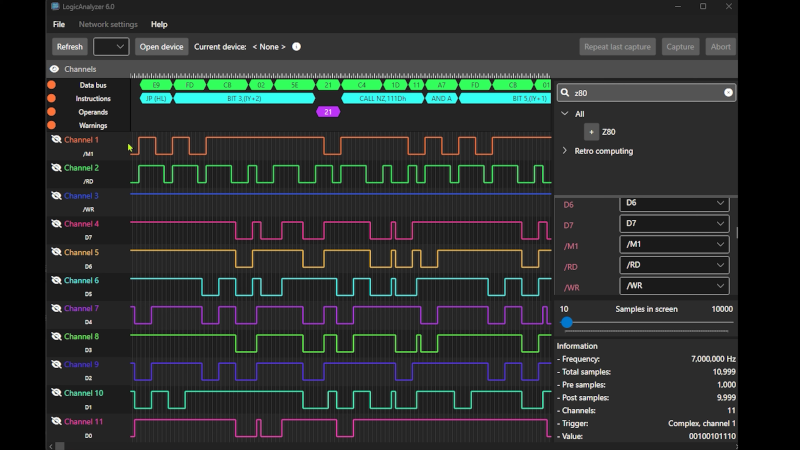
Version 6 included a major overhaul of the project’s analysis application. Improvements included faster waveform rendering, automatic analyzer detection, a terminal-based capture utility, combined software packages, and support for Sigrok protocol decoders.
Sigrok is an open-source signal-analysis framework, while PulseView provides a graphical interface for logic analyzers, oscilloscopes, and mixed-signal instruments. Its decoder library can translate raw transitions into recognizable UART characters, SPI transactions, I2C addresses, and many other protocols. Instead of manually counting pulses, users can inspect decoded bytes and timing information directly.
The project initially used custom analysis software because implementing a dedicated application was easier for its developer than writing and maintaining a Sigrok driver. Later releases gained CSV export, PulseView compatibility, and eventually broad Sigrok decoder integration. That progression gives users the convenience of the project’s own interface while opening the door to an established analysis ecosystem.
What Can You Debug With It?
UART communication
UART debugging is an ideal beginner application. Connect a channel to the transmitter line, share a ground connection, select the expected baud rate, and inspect the decoded characters. A logic analyzer can reveal mismatched baud settings, incorrect polarity, framing errors, missing stop bits, or a device that transmits perfectly while the receiving software listens on the wrong pin.
I2C buses
An I2C capture shows the clock line, data line, device address, read or write direction, acknowledgments, and transferred bytes. This makes it easier to distinguish between a software configuration problem and a hardware device that simply is not responding.
PulseView can automatically associate appropriately labeled SCL and SDA channels with an I2C decoder, reducing setup work. A capture may reveal a missing acknowledgment, a repeated start condition, an incorrect address, or a clock line being held low by a confused peripheral.
SPI flash and displays
SPI typically requires monitoring clock, chip select, controller output, and peripheral output. The Pico Logic Analyzer’s channel count leaves room for reset lines, interrupt pins, and additional chip-select signals.
For example, when an SPI display remains blank, the analyzer can show whether the controller sends initialization commands, whether chip select activates at the correct time, and whether the clock polarity matches the display’s requirements. SparkFun demonstrates similar workflows for observing SPI communication with memory cards and other peripherals.
Retrocomputers and parallel buses
Wide channel counts are useful when examining address lines, data lines, read and write controls, interrupts, and clock signals in older computers. The upgraded analyzer has already attracted interest from ZX Spectrum developers because its 5-volt level shifting and multi-channel capture are well suited to classic hardware.
A parallel decoder can also interpret synchronous or asynchronous buses with selectable data widths and optional control signals. That is much more pleasant than staring at 16 individual traces until the hexadecimal value reveals itself through meditation.
Understanding the 400 MHz Claim
A high sampling rate improves timing resolution, but it does not automatically establish the analyzer’s usable signal bandwidth. Saleae recommends sampling digital signals at least four times faster than their bandwidth. Under that guideline, a 400 MS/s acquisition rate might correspond to a theoretical signal bandwidth near 100 MHz before accounting for the input circuit, probe wiring, threshold behavior, and signal quality.
Professional logic analyzer specifications separately characterize sample rate, channel count, minimum detectable pulse width, input bandwidth, threshold accuracy, channel skew, memory depth, and triggering performance. Tektronix similarly distinguishes digital timing acquisition from the analog behavior of the signal being measured.
Probe construction becomes especially important above tens of megahertz. Long unshielded leads add capacitance, inductance, crosstalk, and ground-loop problems. A waveform may look like a valid logic transition while actually representing ringing picked up by the probe. High-speed measurements benefit from short connections, nearby ground points, suitable termination, and careful board layout.
Therefore, the 400 MS/s mode is best viewed as valuable timing resolution for burst captures and edge placement, not permission to ignore signal integrity. Jumper wires remain wonderful servants but terrible RF engineers.
Limitations to Consider Before Building
- Experimental overclocking: Maximum-speed operation exceeds the RP2350’s official clock specification and may not be stable on every board.
- Finite capture memory: High sample rates consume RAM quickly, limiting capture duration.
- No continuous high-speed streaming: Captures are generally buffered before transfer because USB bandwidth is far below the analyzer’s peak internal sampling rate.
- Digital-only interpretation: The analyzer cannot replace an oscilloscope when voltage shape, ringing, noise, rise time, or overshoot must be measured.
- Probe quality matters: Loose wires can reduce trustworthy high-frequency performance.
- Open-source development: Documentation, software behavior, and experimental firmware may change between releases.
The project repository currently identifies version 6.0.0.1 as the stable release published on February 9, 2025, while also pointing users toward a later 6.5 beta. Version 6 brought official Pico 2 support, redesigned software, automatic device detection, terminal capture tools, and Sigrok decoder compatibility.
How It Compares With Commercial Logic Analyzers
Commercial tools generally provide polished software, calibrated thresholds, protected inputs, better probes, deeper memory, continuous streaming, hardware glitch detection, warranties, and formally tested specifications. High-end models from companies such as Keysight, Tektronix, Digilent, and Saleae can also provide much faster timing acquisition and advanced trigger sequencing.
For example, Digilent’s Digital Discovery supports up to 32 digital channels and high-speed modes reaching 800 MS/s, while professional Keysight platforms extend into multi-gigahertz timing acquisition with large memories and specialized probes. Those products serve a different market and budget.
The Pico Logic Analyzer competes through accessibility, openness, flexibility, and educational value. Users can inspect the firmware, modify the trigger logic, manufacture the PCB, add protocol support, or adapt the design to a specialized project. It is not a calibrated replacement for every professional instrument. It is a remarkably capable platform for the priceand a particularly good way to learn what a logic analyzer is doing rather than treating the enclosure as a box of expensive magic.
Extended Workshop Experience: Using the New Version in Practice
The following is a realistic composite workshop scenario based on common logic-analyzer workflows rather than a claim of one specific laboratory test.
Imagine an RP2040-based controller connected to a small SPI display, an I2C temperature sensor, and a UART debug port. The firmware boots, prints a startup message, and then freezes before the display shows anything useful. Naturally, the first response is to reread the code. The second response is to blame the display. The third response is to make coffee and reconsider every career decision that led to this moment.
The Pico Logic Analyzer changes the investigation from guessing to observing. Four channels go to the SPI clock, chip-select, controller-output, and peripheral-output lines. Two more connect to the I2C clock and data signals, while another channel watches the UART transmitter. Ground is connected close to the target board rather than through a wandering cable stretched across the desk.
The first capture uses a moderate sample rate. This is an important practical habit: the maximum setting is not automatically the best setting. A 10 MHz SPI bus does not require experimental 400 MS/s acquisition just to determine whether initialization commands were transmitted. A lower rate provides a longer capture window and reduces memory pressure.
The trigger is configured on the falling edge of the display’s chip-select line, with part of the buffer reserved for samples before the trigger. That pre-trigger history becomes immediately useful. The display transaction is present, but an I2C transaction occurs several microseconds earlier and ends without an acknowledgment. The processor retries the sensor read repeatedly, blocking the program before the display initialization routine completes.
The raw waveforms already tell a useful story, but protocol decoding saves time. The I2C decoder identifies the transmitted address and marks the missing acknowledgment. A quick comparison with the sensor documentation reveals that the firmware uses the eight-bit address copied from a datasheet table, while the software library expects the seven-bit form.
After correcting the address, another capture confirms that the sensor acknowledges properly. The SPI decoder now displays the initialization bytes sent to the screen. Unfortunately, the display still remains blank. This time the timing diagram reveals that chip select returns high between bytes even though the display controller expects it to remain low for the complete command sequence.
A firmware adjustment fixes the transaction framing. The next capture shows the expected command and data sequence, and the display finally lights. No components were replaced. No random delay statements were sprinkled through the code like electronic seasoning. The analyzer simply showed what the system was actually doing.
The high-speed mode becomes more relevant during a later test involving a narrow interrupt pulse. At a low sample rate, the pulse appears inconsistently or disappears between sample points. Increasing the acquisition rate provides finer timing resolution and confirms that the interrupt line is active for only a few tens of nanoseconds. The capture does not measure the analog quality of that pulse, but it reveals enough digital timing information to explain why the microcontroller occasionally misses it.
This experience illustrates the new Pico Logic Analyzer’s greatest strength. Its value is not simply the maximum number printed beside “MS/s.” The real benefit comes from combining multiple channels, useful triggers, pre-trigger history, protocol decoding, adjustable voltage levels, and an open design. It turns debugging from a debate with the schematic into a conversation with the hardwareand, unlike the schematic, the hardware usually tells the truth.
Final Takeaway
The new Pico Logic Analyzer represents a substantial step forward for affordable digital debugging. Its single-board design is cleaner, Pico 2 support expands memory and processing resources, configurable level shifting broadens compatibility, and daisy chaining makes unusually wide captures possible. Version 6’s software overhaul and Sigrok decoder support may ultimately prove even more valuable than the headline-grabbing experimental 400 MS/s mode.
It is still a maker-oriented instrument rather than a fully characterized professional analyzer. Maximum-speed operation relies on out-of-spec overclocking, capture depth remains finite, and reliable high-frequency measurements demand careful probing. Within those boundaries, however, the project delivers an impressive combination of performance, openness, and practical usefulness.
Note: The 400 MS/s figure describes an experimental sampling configuration reported by the project, not a guaranteed 400 MHz measurement bandwidth. Builders should consult the current repository documentation, release notes, hardware files, and RP2350 specifications before assembling or operating the analyzer at elevated clock speeds or voltages.