There is something wonderfully rebellious about looking inside a microcontroller that normally spends its life hidden under a tiny black plastic roof. The PIC12F683 is an 8-pin workhorse that has powered hobby projects, small appliances, sensor circuits, LED controllers, battery-powered gadgets, and countless “I only need one more GPIO pin” situations. From the outside, it looks like a modest little package. Inside, it is a carefully organized CMOS city with memory blocks, power rails, analog circuitry, digital logic, bond pads, and more microscopic real estate drama than most people expect.
Decapsulating a PIC12F683 is not about turning a chip into expensive electronic confetti. Done responsibly in a professional or properly equipped educational setting, it can help researchers, repair analysts, semiconductor students, and hardware historians examine how a low-cost microcontroller is physically implemented. The goal is not simply to admire shiny metal traces. The real fun begins when you compare what you see under magnification with the device datasheet, block diagram, pinout, memory map, and peripheral list.
This article explores how a PIC12F683 decapsulation project can reveal clues about CMOS implementation, memory organization, analog layout, power distribution, and semiconductor design priorities. It also explains what a die photograph can tell you, what it cannot tell you, and why the phrase “I can probably do this on my kitchen counter” should make everyone in the room slowly back away from the chemicals.
Why the PIC12F683 Is Such an Interesting Chip to Examine
The PIC12F683 is a compact 8-bit PIC microcontroller with a 2K x 14-bit Flash program memory, 128 bytes of RAM, 256 bytes of data EEPROM, timers, a comparator, a 10-bit ADC, an internal oscillator, and a Capture/Compare/PWM module. That is a surprising amount of functionality for an 8-pin device. It is small enough to feel approachable, yet complex enough to make a die photo look like a metropolitan transit map designed by ants with engineering degrees.
The datasheet block diagram is especially useful because it provides a logical map before you ever look at the silicon. It identifies major functions such as Flash program memory, RAM, EEPROM, analog-to-digital conversion, comparator circuitry, oscillator logic, timers, power-on reset, brown-out reset, watchdog circuitry, and the CPU core. A decapsulated die gives you the physical counterpart to that logical diagram.
That comparison is where the educational value lives. The block diagram says, “Here is the Flash memory.” The die photograph asks, “Can you identify the large repetitive block that behaves like memory?” The datasheet says, “Here is the analog comparator.” The die image asks, “Why might the analog area use different spacing, shielding, and geometry than the compact digital logic?”
What Decapsulation Actually Means
Decapsulation is the process of removing or opening the protective package material around an integrated circuit so the die, bond wires, lead frame, and bonding pads can be inspected. In a plastic-packaged microcontroller, the silicon die is normally embedded in epoxy molding compound. Removing that material exposes the top of the die, but it does not automatically reveal every transistor, every memory cell, or every manufacturing secret.
A top-side decapsulation can reveal bond wires, bond pads, top-level metal routing, power structures, large capacitor arrays, and broad layout regions. To see deeper transistor-level details, an analyst may need controlled delayering and specialized imaging. That is a different level of work entirely. It is slower, more destructive, and much easier to get wrong. Semiconductor analysis is one of those disciplines where “just one more step” can become “well, that used to be a chip.”
Professional failure-analysis workflows often begin with non-destructive inspection before any package is opened. X-ray imaging can help evaluate bond-wire placement and package structure, while acoustic imaging can reveal delamination or internal voids. Decapsulation is usually performed only after the analyst understands what they are trying to inspect and why. That approach is smarter than opening first and asking questions later.
Understanding the PIC12F683 CMOS Implementation
CMOS Is More Than “Tiny Transistors”
CMOS stands for complementary metal-oxide-semiconductor. At a high level, it uses complementary NMOS and PMOS transistors to implement digital logic efficiently. In a CMOS microcontroller, the silicon substrate contains carefully patterned regions for transistors, resistors, capacitors, protection structures, analog circuits, memory cells, and metal interconnects. These structures are layered like a very expensive semiconductor lasagna, except nobody is allowed to eat it.
When viewing a decapsulated die from the top, the most visible features are often the upper metal layers and passivation. The active transistor regions sit deeper in the stack. A CMOS layout can include diffusion regions, polysilicon gates, contacts, vias, wells, and multiple metal routing layers. In academic CMOS layout examples, the visual language of a chip is built from these repeating layers: active areas define transistor regions, polysilicon often forms gates, and metal layers distribute power and signals across the die.
How to Read the Die Like a Semiconductor Detective
A die image rarely comes with helpful labels such as “Hello, I am the EEPROM.” Instead, you identify functions by pattern, location, scale, symmetry, and connectivity. Large regular arrays are usually strong candidates for memory. Wide metal paths often indicate power distribution. Peripheral structures near bond pads may be I/O cells, protection circuitry, or pad drivers. Areas with generous spacing, repeated matched devices, or routing away from noisy digital regions may be analog circuitry.
Memory blocks often look disciplined and repetitive because memory cells are repeated many times. CPU logic, by contrast, can look more irregular because it contains instruction decoding, arithmetic functions, control logic, register handling, stack control, and timing circuitry. Analog sections can appear surprisingly spacious compared with digital logic. That is not because analog engineers dislike efficiency. It is because analog circuits care deeply about matching, noise, parasitic effects, voltage references, and keeping noisy switching circuitry from throwing a tiny electrical party next door.
At the outer edge of the die, you may find large bond pads connected to the package leads. These pads are much larger than internal logic features because they must support wire bonding and tolerate mechanical handling. Near them, CMOS I/O structures usually include protection devices and output drivers. The PIC12F683 has multiple alternate pin functions, including analog inputs, comparator connections, programming pins, oscillator functions, and digital GPIO roles, so its I/O regions must support more than simple on-or-off behavior.
What Published PIC12F683 Die Analysis Reveals
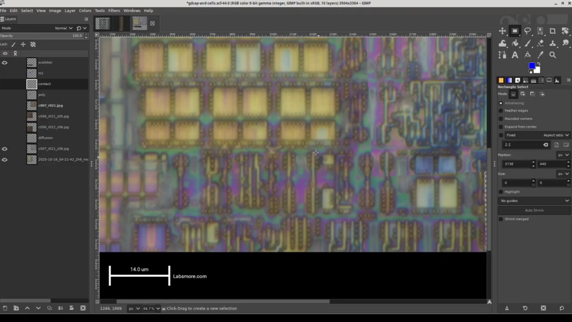
A published teardown of the PIC12F683 described a physical floor plan that aligns well with the microcontroller’s documented features. The analysis identified a large Flash memory region near the lower center of the die, RAM to one side, EEPROM above the RAM, configuration-related memory nearby, and analog circuitry arranged along the upper and right-side portions of the die. The teardown also described visible capacitor structures associated with high-voltage generation for nonvolatile memory operations.
That floor plan makes practical sense. Flash memory and EEPROM need special circuitry for program and erase operations, including voltage-generation support. RAM is physically different because it is volatile and does not require the same charge-storage behavior as nonvolatile memory. Analog functions such as comparators and ADC-related circuitry benefit from physical separation from aggressive digital switching zones. A designer cannot put every block wherever there happens to be empty silicon. Noise, routing, test access, power delivery, and manufacturing rules all have a vote.
A third-party teardown also estimated that the PIC12F683 used a process around the mid-2000s generation of CMOS technology with multiple metal layers. That should be treated as an informed visual interpretation rather than a manufacturer-confirmed process disclosure. Still, the visible organization offers an excellent example of how a modest microcontroller combines digital logic, nonvolatile memory, analog peripherals, and power-management circuitry on one small die.
Matching Physical Regions to the PIC12F683 Block Diagram
Flash Program Memory
The PIC12F683 implements 2K words of 14-bit program memory. In a die image, the Flash array is likely to appear as a large regular block because it contains repeated memory structures. The surrounding circuitry may include row and column decoding, sense-related circuits, program control logic, and high-voltage support. The physical size of this region reflects an important truth about older microcontrollers: memory often consumes more die area than the CPU logic that executes the instructions.
RAM and EEPROM
RAM and EEPROM serve very different purposes, and their physical layouts reflect that difference. RAM is optimized for fast temporary storage while the chip is powered. EEPROM is designed to retain data without power. A PIC12F683 die examination can help illustrate why these two storage technologies are not simply interchangeable boxes drawn on a block diagram. One is fast and forgetful. The other is persistent and occasionally stubborn, much like a coworker who remembers every meeting from 2017.
Analog Peripherals
The PIC12F683 includes a 10-bit ADC, analog comparator, and programmable reference functions. Analog regions may be recognized by their relative separation from dense digital routing, their use of matched geometry, and their proximity to analog-capable I/O pads. A die photograph cannot prove every transistor-level function by itself, but it can reveal where the designers likely gave analog circuitry room to breathe.
Clock, Reset, and Power Management
The internal oscillator, power-on reset, brown-out detection, watchdog timer, and timing circuits are all critical to the microcontroller’s operation. These blocks may not be visually obvious in a top-level die photo because they are smaller and more integrated into the logic fabric. However, the device documentation confirms their presence, allowing an analyst to narrow down likely regions by comparing layout placement with known memory, analog, and I/O areas.
What You Can Learn From a Decapsulated PIC12F683
A decapsulated microcontroller can teach several useful lessons. First, software architecture and silicon architecture are related but not identical. A programmer may think of the PIC12F683 as registers, instructions, GPIO, timers, and interrupts. A die analyst sees memory arrays, metal rails, bond pads, capacitor structures, analog blocks, and repeated transistor-level patterns.
Second, the die helps explain product trade-offs. The PIC12F683 is not a giant, highly parallel processor. It is a compact, cost-conscious controller designed to provide enough Flash, EEPROM, analog capability, timing resources, and I/O flexibility for embedded applications. Its implementation reflects that mission. The design is dense where it needs to be dense, conservative where reliability matters, and practical everywhere else.
Third, die analysis helps build respect for manufacturing. A microcontroller that costs only a few dollars can contain thousands of carefully aligned structures, multiple functional layers, nonvolatile memory technology, analog peripherals, and electrical protection circuits. That tiny DIP package may look like it belongs in a beginner’s breadboard kit, but inside it is still the result of an industrial semiconductor process that makes a sandwich press look embarrassingly underqualified.
What a Die Photograph Cannot Tell You
A die image is powerful, but it is not magic. It cannot automatically reveal source code, exact transistor sizing, complete routing connectivity, every fabrication parameter, or every security feature. It also cannot reliably identify a transistor-level circuit without additional work, careful imaging, cross-checking, and often controlled delayering.
It is especially important not to confuse educational observation with a reason to defeat firmware protection or extract proprietary code. Responsible hardware research focuses on authorized devices, obsolete hardware, self-owned samples, coursework, quality analysis, reliability investigations, and transparent experimentation. A PIC12F683 is a fine subject for learning about layout and CMOS design without crossing ethical or legal boundaries.
Safety and Ethical Boundaries Matter
Decapsulation can involve hazardous materials, specialized equipment, electrical risks, optical hazards, waste handling, and fragile semiconductor structures. It is not appropriate as a casual home experiment. Professional laboratories use controlled processes, protective equipment, ventilation, chemical handling procedures, and inspection workflows designed to minimize risk to both people and samples.
Even when safety equipment is available, a decapsulated device should be treated as a specimen rather than a guaranteed working microcontroller. Bond wires can be damaged, passivation can be affected, and exposed surfaces can be contaminated. Electrical checks before and after analysis are valuable because they distinguish “the chip was already faulty” from “the chip became a tiny museum exhibit during inspection.”
Conclusion: A Tiny PIC, a Big CMOS Lesson
Decapsulating a PIC12F683 to examine its CMOS implementation is a fascinating way to connect embedded programming with semiconductor physics. The chip’s logical block diagram becomes a physical map of Flash, RAM, EEPROM, analog circuitry, I/O structures, power routing, and control logic. It turns an ordinary microcontroller into a visual lesson in CMOS design, manufacturing discipline, and engineering trade-offs.
The PIC12F683 may be small, but it is not simple. Its die demonstrates how much engineering can fit into a low-pin-count controller: nonvolatile memory, analog sensing, timing, digital logic, clocking, reset behavior, protection structures, and programmable control. Looking inside does not replace the datasheet. It makes the datasheet come alive.
Field Notes: Lessons From PIC12F683 CMOS Examination
One of the most common surprises in PIC12F683 die analysis is how quickly the scale becomes disorienting. On a breadboard, the chip feels almost toy-like. Under magnification, the same device becomes a landscape of metallic roads, oddly shaped districts, and microscopic apartment blocks for electrons. The first useful lesson is to avoid trying to understand everything at once. Start with the perimeter, identify the bond pads, locate the largest repeating regions, and then compare the physical map with the datasheet block diagram.
Another recurring lesson is that photographs can be misleading when viewed without context. Reflective metal layers, passivation, shadows, uneven illumination, and optical depth can make a region look like a different material or functional block than it actually is. A large bright area may be a metal plane. A dark area may simply be a change in focus. Good analysis depends on several images, scale references, documented orientation, and comparisons with known layout behavior. One dramatic photo may win attention online, but a carefully documented image set wins confidence.
Bond wires deserve respect because they are both informative and fragile. They reveal how the package leads connect to the die, and they can help identify power pins, ground pins, programming pins, and signal connections. At the same time, they are delicate enough that rough handling can turn a useful sample into a silent one. That is why professional analysis often values non-destructive inspection before decapsulation. It is easier to understand a wire bond after seeing where it used to be than after it has vanished into the realm of “probably fine until I touched it.”
A useful habit is to treat the datasheet as a legend for the die photograph. The PIC12F683 documentation identifies the program memory, EEPROM, RAM, oscillator, comparator, timers, ADC, reset functions, and GPIO roles. The physical die should be interpreted against those known functions, not guessed from visual pattern alone. A repetitive block may strongly suggest memory, but the memory type should be supported by location, nearby support circuitry, and the device architecture. Good reverse engineering is less about declaring certainty and more about building confidence from independent clues.
The analog portion of a small microcontroller is often more interesting than the digital core because it demonstrates the practical realities of mixed-signal design. Digital logic can tolerate dense switching and aggressive routing. Analog circuitry usually needs cleaner references, controlled geometry, lower noise coupling, and physical separation from fast-changing signals. When examining a PIC12F683 die, it is reasonable to expect the analog-related region to look less like a dense grid and more like a carefully spaced neighborhood where everyone complains about noise after 9 p.m.
Finally, the biggest lesson from a PIC12F683 teardown is that semiconductor design rewards patience. It is tempting to jump directly from a die photograph to bold claims about transistor counts, fabrication nodes, security features, or hidden functions. A more disciplined approach is better: verify the device revision, document the package, compare multiple samples when possible, map obvious blocks first, and state uncertainty clearly. That mindset makes the analysis more useful, more credible, and much more educational than a dramatic guess dressed up as certainty.
Technical research basis: PIC12F683 device documentation and block diagram: . CMOS layout layers and device structures: . Destructive physical inspection and decapsulation context: . Failure-analysis imaging and wire-bond inspection context: . PIC12F683 die-floor-plan observations: .